Quality supplier of advanced semiconductors with international leadership position
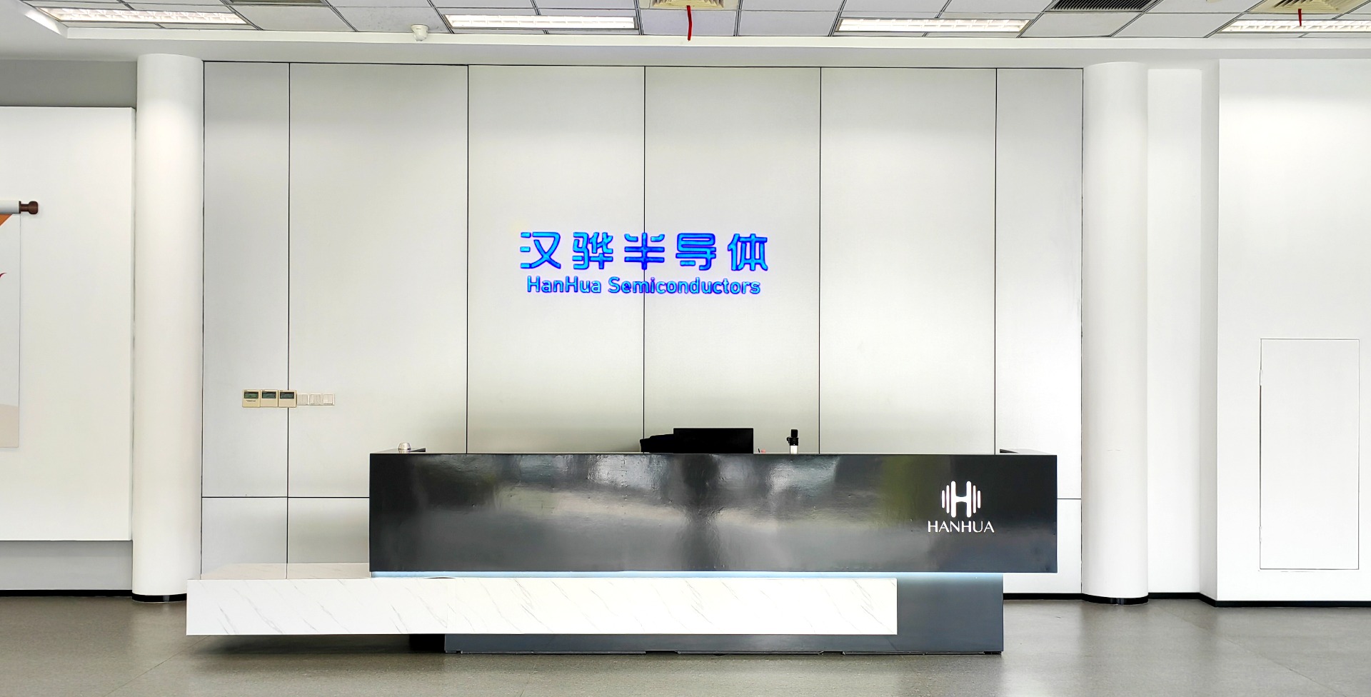
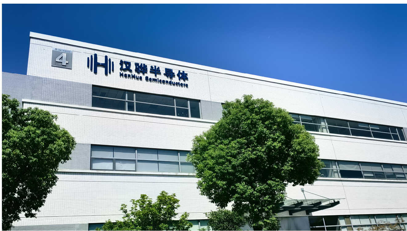
- Hanwha Semiconductor was launched in 2017 by the Yangtze River Delta National Innovation Center and Suzhou Industrial Park as the cornerstone investors, together with the founding team of Hanwha Semiconductor.
HanHua Semiconductor was launched by the Yangtze River Delta National Innovation Center and Suzhou Industrial Park as the cornerstone investor and the founding team, which is the first forward-looking, disruptive and major R&D project supported by China's innovative method of "allocation and investment combination".
It is the first time that China adopts the innovative method of "allocation and investment combination" to support forward-looking and disruptive R&D projects.
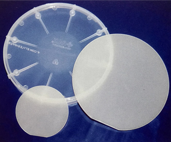
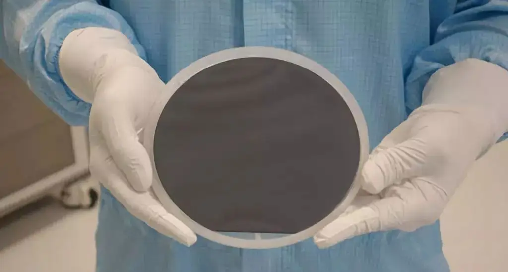
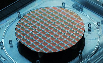
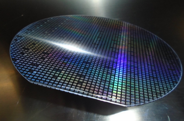
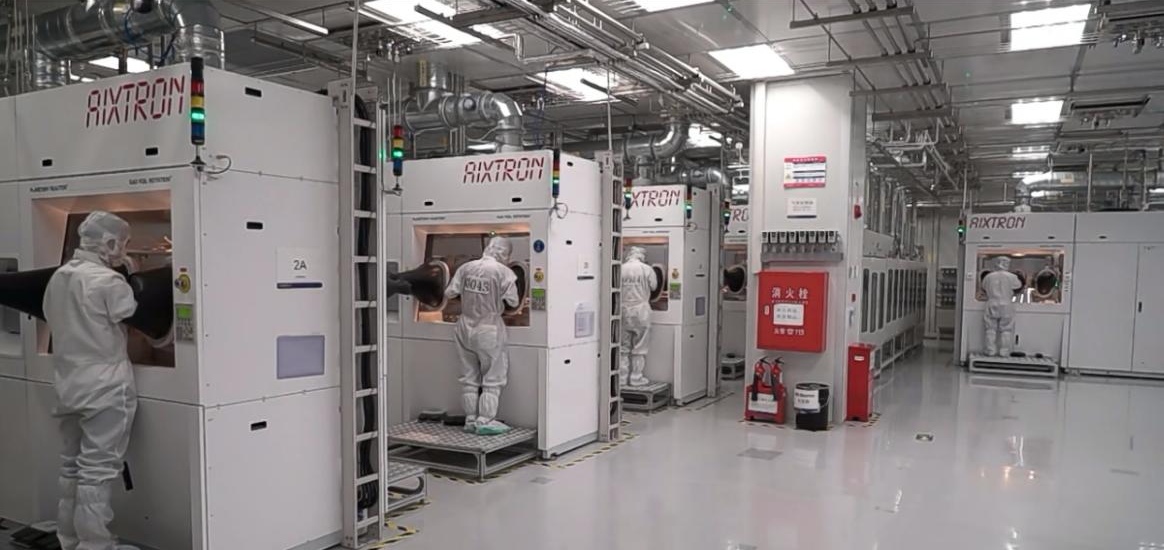
- At present, the company has built a 20,000 square meter factory in the core area of Suzhou Industrial Park, with an annual production capacity of about 300,000 pieces of 4/6/8-inch compatible high-end chips.
4/6/8-inch compatible high-end GaN material production line and 8-inch 3DIC Hybrid Bonding chip production line.
It is a high-end semiconductor closed-loop R&D and large-scale production base with international leading standard, and is also the largest independent production base in China.
It is also the largest independent gallium nitride epitaxial supplier with the largest production capacity in China.
- Hanwa has applied for about 100 domestic and foreign patents, and more than 40 patents have been approved. Since its establishment, HanHua has been honored as one of the
Since its establishment, HanHua has been honored as a national specialized, specialized and new small giant, a national high-tech enterprise, a national potential unicorn, a double innovation team of Jiangsu Province, a major innovation team of Gusu, and a Suzhou industrial enterprise,
Gusu Major Innovation Team, Suzhou Industrial Park Major Leader and other honors.